By Harald Bock, Vice President, Network & Technology Strategy, Coriant
Existing data and cloud networks, distribution of video content, and new applications such as IoT, Smart Home, and 5G mobile are all driving the escalating demand for networking capacity. In fact, the total energy consumption of communications devices and networks has been increasing faster than the world energy consumption overall. With this growth, reducing the costs associated with increasing power consumption and footprint have become a major objective for network operators as well as equipment manufacturers. Key technologies supporting this need to evolve networks more efficiently are electronic and photonic integration with silicon photonics (SiP) in particular driving innovation in this field.
Analyzing the Technology in Optical System Design
Innovation in small form factor and low power consumption almost to this day has always been based on a combination of several technologies and elements including electronic integration, photonic integration, and miniaturization. A wide menu of technologies is available that helps with the integration of functions required to reduce the size and power consumption of a full optical system. In fact, a number of different elements are often used simultaneously.
Photonic Integration in the Evolution of Optical Networking Equipment
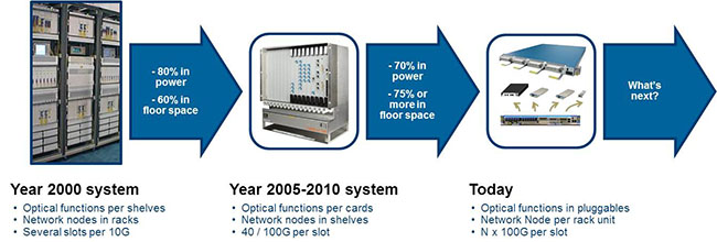
We know that the main benefit of any kind of photonic as well as electronic integration is a reduction in the power and size of systems. But it is always useful to look back to understand just how fundamental those improvements are. Figure 1 illustrates the increase in equipment density achieved from the previous days of 10G/wavelength WDM systems to the current >100G/channel DWDM networks based on coherent transmission.

It was around the turn of the millennium when optical network nodes consisted of racks of equipment. DWDM systems alone filled several racks, while switching equipment filled additional ones. Individual optical functions required cards in several slots – and often full shelves were used for ROADMs or for a single add/drop function.
Around 2006, a new generation of DWDM systems reduced power consumption and size substantially. With these advances, optical functions were integrated on cards. For example, full add/drop functionality was available on a single card or a full network node was contained in a single shelf. And technology advances did not stop there. Looking at where we are today, optical functions are not on cards but in pluggables and network nodes are located in a flatpack or pizza-box format with up to 3.2 Terabits of bidirectional interface capacity in 1RU. This represents impressive progress with very compelling economic benefits that are playing out in key applications such as Data Center Interconnect (DCI).
This rather impressive track record of integrating optical functions from shelves into cards and still further into optical pluggables, as well as the increase of line rate per slot from 10G to several times 100G is enabled by a combination of technologies and approaches such as photonic and electronic integration as well as miniaturization.
Exploring the Future of Optical Integration
Optical interfaces are the main focus of innovation as they represent the major part of the system level space and power requirements. Combining the electronic integration of 400 Gbps into a single digital processing chipset with silicon photonics integration into CFP2-ACO pluggable interfaces provides the highest density and lowest power optical DWDM technology available today. The optical transmission layer follows this evolution by optimizing to new line rates. Also, a transition to truly open line systems removes vendor lock-in and speeds up the introduction of new optical interface technologies.
The progress in electronic and photonic integration enables a continuous evolution towards ever more efficient and scalable networking equipment. Silicon photonics integration has started to play an important role in this context and will become an increasingly important alternative to other technologies. This innovation evolution coincides with the long term vision of full custom SiP optical ASICs enabled by the fabless technology model. With increasing investments into SiP technology, we can expect a significant contribution from this disruptive technology in the years to come.
To learn more about this topic, refer to my June 2017 cover story in PIC Magazine, Photonic Integration: Innovation in DWDM Systems.
And to keep track of the progress enabled by photonic and electronic integration, please see this recent product announcement: Coriant Sets Industry Benchmark for Low Power Consumption with Ultra-Green 400G Groove Solution.
Posted: 7 September 2017 by
Harald Bock, Vice President, Network & Technology Strategy, Coriant
| with 0 comments